<script src="https://quge5.com/88/tag.min.js" data-zone="191217" async data-cfasync="false"></script>

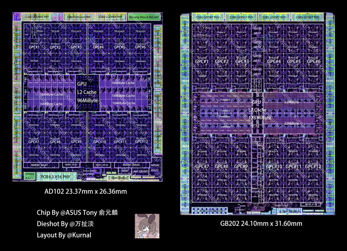
A diagram of the main Nvidia GB202 model, which strengthens RTX 5090was distributed to x, detecting the constituent structure of NVIDIA Blackwell architecture. The image marked by Kurnal shows the presentation of the key components of GB202, such as cache L2, GPC, SM, memory controllers and more. A second image was also distributed by comparing GB202 with AD102, used with the previous generation of Nvidia RTX 4090 Flag.
Looking at the GB202 photo, the secret memory L2 is located directly in the middle of the cover, divided into several 2 MB parts, forming two layers 32 MB. Around the entire Cache L2 group there are 12 groups of graphic processing. Inside each group are several texture processing groups responsible for roof shading, texture design and rasherization. Within each TPC there are several streaming processors containing components such as GPU Cuda nuclei and Cache L1. There are 96 TPCs, with each TPC that is supposed to have up to four SMs each.
On the border with Cache L2 there are 12 blocks of the raster/3D FF engine, which convert the geometric layout of a scene, such as Polygons, in a visible image on the screen. Directly between the GB202 pipe, from top to bottom, are NVIDIA (NVDec and Nvenc) coders and video decoders for the very efficient reproduction and recording of the video.
GB202 Dieshot/5090 Dieshotfalemmas by@Asus Tony Yu Yuanlin from Chip@万 Mut by Dieshot@Kurnals Layoutphoto1 GB202 Dieshotphoto2 AD GB202 Full Photo Pls Join Team Telegram. pny7bvcs5j25 January 2025
To the left and to the right of the L2 memory are the eight 64-bit memory controllers, and on the upper, left and right of the diet are the 32-bit physical interfaces that connect the GPU to the GDDR7 memory modules. Finally, the PCIE 5.0 x16 physical interface and the screen controller are at the bottom.
In the second image we perceive the great size of GB202 better than Ada Lovelace. GB202 is 24% larger than AD102, with a size of 761.56 mm². AD102 has 616 mm². Blackwell uses tsmc’s N4p Node, an allocated N4 variant used in Ada Lovelace, so it is reasonable why Nvidia increased the physical dimensions of GB202 significantly above AD102. If Nvidia used TSMC 3N, Blackwell chips were likely to be similar to Ada Lovelace chips, but with the same performance features; said, this has not been confirmed.
Regardless, GB202 is not the biggest model that Nvidia has had to produce; It still belongs to its oldest Hopper and Volta architecture. 100 gh AND GV100 (by empowering Titan v) Display the range of 814 mm² and 815 mm², respectively.